1. Principles of Silica Sol Chemistry and Colloidal Stability
1.1 Structure and Bit Morphology
(Silica Sol)
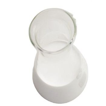
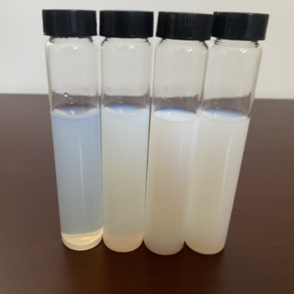
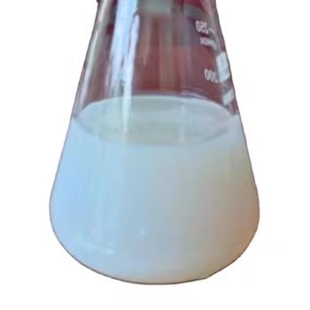
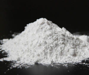
Silica sol is a stable colloidal diffusion consisting of amorphous silicon dioxide (SiO ₂) nanoparticles, normally varying from 5 to 100 nanometers in diameter, suspended in a fluid stage– most frequently water.
These nanoparticles are composed of a three-dimensional network of SiO ₄ tetrahedra, forming a porous and highly reactive surface area rich in silanol (Si– OH) groups that govern interfacial behavior.
The sol state is thermodynamically metastable, preserved by electrostatic repulsion between charged particles; surface cost emerges from the ionization of silanol teams, which deprotonate above pH ~ 2– 3, generating adversely charged fragments that fend off one another.
Fragment form is usually round, though synthesis problems can affect gathering propensities and short-range ordering.
The high surface-area-to-volume proportion– commonly surpassing 100 m ²/ g– makes silica sol exceptionally reactive, making it possible for strong interactions with polymers, steels, and organic particles.
1.2 Stabilization Devices and Gelation Change
Colloidal stability in silica sol is primarily controlled by the equilibrium in between van der Waals eye-catching pressures and electrostatic repulsion, explained by the DLVO (Derjaguin– Landau– Verwey– Overbeek) concept.
At reduced ionic stamina and pH worths over the isoelectric factor (~ pH 2), the zeta potential of fragments is completely adverse to prevent gathering.
However, addition of electrolytes, pH adjustment towards nonpartisanship, or solvent dissipation can evaluate surface area fees, lower repulsion, and trigger fragment coalescence, resulting in gelation.
Gelation entails the development of a three-dimensional network with siloxane (Si– O– Si) bond development in between adjacent bits, transforming the liquid sol right into a rigid, permeable xerogel upon drying out.
This sol-gel transition is relatively easy to fix in some systems yet commonly causes irreversible architectural adjustments, developing the basis for advanced ceramic and composite manufacture.
2. Synthesis Paths and Process Control
( Silica Sol)
2.1 Stöber Approach and Controlled Growth
One of the most widely recognized technique for producing monodisperse silica sol is the Stöber procedure, developed in 1968, which includes the hydrolysis and condensation of alkoxysilanes– normally tetraethyl orthosilicate (TEOS)– in an alcoholic medium with aqueous ammonia as a driver.
By specifically managing parameters such as water-to-TEOS ratio, ammonia focus, solvent composition, and reaction temperature level, bit size can be tuned reproducibly from ~ 10 nm to over 1 µm with narrow dimension distribution.
The mechanism proceeds through nucleation complied with by diffusion-limited development, where silanol teams condense to develop siloxane bonds, developing the silica structure.
This method is suitable for applications requiring uniform round particles, such as chromatographic supports, calibration standards, and photonic crystals.
2.2 Acid-Catalyzed and Biological Synthesis Routes
Alternative synthesis techniques consist of acid-catalyzed hydrolysis, which prefers direct condensation and results in more polydisperse or aggregated bits, frequently used in commercial binders and coverings.
Acidic problems (pH 1– 3) advertise slower hydrolysis however faster condensation between protonated silanols, bring about uneven or chain-like structures.
A lot more lately, bio-inspired and environment-friendly synthesis methods have emerged, making use of silicatein enzymes or plant extracts to speed up silica under ambient conditions, reducing energy intake and chemical waste.
These lasting techniques are obtaining passion for biomedical and ecological applications where pureness and biocompatibility are critical.
Furthermore, industrial-grade silica sol is commonly produced via ion-exchange processes from sodium silicate options, adhered to by electrodialysis to get rid of alkali ions and maintain the colloid.
3. Practical Properties and Interfacial Habits
3.1 Surface Reactivity and Adjustment Techniques
The surface of silica nanoparticles in sol is controlled by silanol teams, which can take part in hydrogen bonding, adsorption, and covalent grafting with organosilanes.
Surface adjustment making use of coupling agents such as 3-aminopropyltriethoxysilane (APTES) or methyltrimethoxysilane introduces useful teams (e.g.,– NH TWO,– CH THREE) that alter hydrophilicity, reactivity, and compatibility with organic matrices.
These alterations enable silica sol to serve as a compatibilizer in crossbreed organic-inorganic compounds, boosting diffusion in polymers and boosting mechanical, thermal, or obstacle residential properties.
Unmodified silica sol exhibits solid hydrophilicity, making it optimal for aqueous systems, while modified variations can be dispersed in nonpolar solvents for specialized coatings and inks.
3.2 Rheological and Optical Characteristics
Silica sol dispersions normally exhibit Newtonian circulation behavior at low focus, but thickness rises with bit loading and can move to shear-thinning under high solids content or partial gathering.
This rheological tunability is made use of in coatings, where controlled circulation and leveling are essential for uniform movie development.
Optically, silica sol is clear in the visible spectrum as a result of the sub-wavelength dimension of bits, which lessens light spreading.
This transparency permits its usage in clear finishings, anti-reflective movies, and optical adhesives without endangering aesthetic quality.
When dried out, the resulting silica film maintains transparency while offering solidity, abrasion resistance, and thermal stability up to ~ 600 ° C.
4. Industrial and Advanced Applications
4.1 Coatings, Composites, and Ceramics
Silica sol is extensively utilized in surface area coatings for paper, fabrics, steels, and building and construction products to enhance water resistance, scrape resistance, and durability.
In paper sizing, it boosts printability and dampness obstacle homes; in shop binders, it replaces organic materials with environmentally friendly inorganic options that decay cleanly throughout casting.
As a precursor for silica glass and ceramics, silica sol enables low-temperature construction of thick, high-purity components via sol-gel handling, avoiding the high melting factor of quartz.
It is also employed in investment casting, where it develops solid, refractory molds with great surface area coating.
4.2 Biomedical, Catalytic, and Power Applications
In biomedicine, silica sol acts as a system for medication delivery systems, biosensors, and diagnostic imaging, where surface area functionalization enables targeted binding and regulated launch.
Mesoporous silica nanoparticles (MSNs), stemmed from templated silica sol, supply high filling ability and stimuli-responsive release systems.
As a stimulant support, silica sol supplies a high-surface-area matrix for paralyzing steel nanoparticles (e.g., Pt, Au, Pd), boosting dispersion and catalytic effectiveness in chemical transformations.
In energy, silica sol is made use of in battery separators to improve thermal stability, in gas cell membrane layers to enhance proton conductivity, and in photovoltaic panel encapsulants to protect versus wetness and mechanical stress.
In summary, silica sol stands for a fundamental nanomaterial that connects molecular chemistry and macroscopic capability.
Its manageable synthesis, tunable surface chemistry, and versatile handling allow transformative applications across sectors, from lasting production to sophisticated health care and power systems.
As nanotechnology progresses, silica sol remains to act as a model system for creating wise, multifunctional colloidal products.
5. Supplier
Cabr-Concrete is a supplier of Concrete Admixture with over 12 years of experience in nano-building energy conservation and nanotechnology development. It accepts payment via Credit Card, T/T, West Union and Paypal. TRUNNANO will ship the goods to customers overseas through FedEx, DHL, by air, or by sea. If you are looking for high quality Concrete Admixture, please feel free to contact us and send an inquiry.
Tags: silica sol,colloidal silica sol,silicon sol
All articles and pictures are from the Internet. If there are any copyright issues, please contact us in time to delete.
Inquiry us


: A Multifunctional Refractory Ceramic Bridging Electronic, Thermoelectric, and Neutron Shielding Technologies calcium boride")